In RF research and engineering, ultra-wideband RF signal record playback systems are often used to fully capture on-site electromagnetic signals for post-analysis or to replay the electromagnetic environment back in the lab. For ultra-wideband signals with an instantaneous bandwidth exceeding 500MHz, record-and-playback encounters a particularly large data throughput problem – what we also call the high-throughput challenge.
Core Challenges of Ultra-Wideband RF Record & Playback
Take a common X‑band radar as an example. Suppose its operating frequency range is 9 GHz to 10 GHz. If you want to record all signals in this band, the instantaneous bandwidth to be recorded is 1 GHz. To generate a baseband signal from this 1 GHz data bandwidth, you must first apply shaping filtering. This shaping filtering ensures that the signal experiences no inter‑symbol interference and has sufficiently good out‑of‑band rejection. Therefore, when capturing, we actually acquire a slightly larger bandwidth than the signal itself. The ratio of this extra bandwidth is called the roll‑off factor. Typically, the roll‑off factor is between 0.2 and 0.25. If I take a roll‑off factor of 0.2, then a signal with 1 GHz instantaneous bandwidth corresponds to a Nyquist bandwidth of 1.2 GHz. This bandwidth is numerically equal to the I/Q rate. So the I/Q rate of the captured signal is also 1.2 G samples per second. Each I/Q pair corresponds to two sample points. If the ADC resolution is 14 bits, each sample point requires two bytes for storage. As a result, each I/Q pair needs four bytes to store. The I/Q rate of 1.2 G samples per second translates to a data rate of 4.8 GB per second.
9-10GHz X-band signal transmission relies on Rectangular Straight Waveguide or Double Ridge Straight Waveguide for stable signal transmission in radar test setup.
Thus, if we want to capture a 1 GHz instantaneous bandwidth signal on two channels, the data volume reaches 9.6 GB per second. For four channels with 400 MHz instantaneous bandwidth each, the data volume reaches 8 GB per second. For a single channel with 2 GHz instantaneous bandwidth, the data volume reaches 10 GB per second. Such huge data volumes place great pressure on disks, data buses, and even memory.
Ultra-Wideband RF Record & Playback: NVMe SSD Storage Speed Limitation
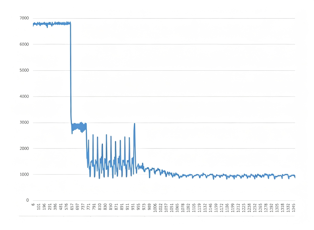
To record and replay ultra‑wideband RF signals, a high‑throughput disk writing capability of 8‑10 GB per second is required. Many NVMe SSDs on the market claim write speeds of nearly 7 GB per second. So wouldn’t two such drives be enough? Actually, not at all. Real‑world tests on these drives show that their initial speed is very high, but after a period of time, the speed drops dramatically – even down to only about 1 GB per second. If we put four such drives into a RAID 0 array (the fastest mode), the maximum write speed is only about 4 GB per second. But as we already noted, we need 8‑10 GB per second, so this does not meet the requirement.
High-power radar input requires Coaxial Fixed Attenuator to protect front-end acquisition hardware; unused test ports should install Coaxial Termination to avoid reflected signal error during recording.
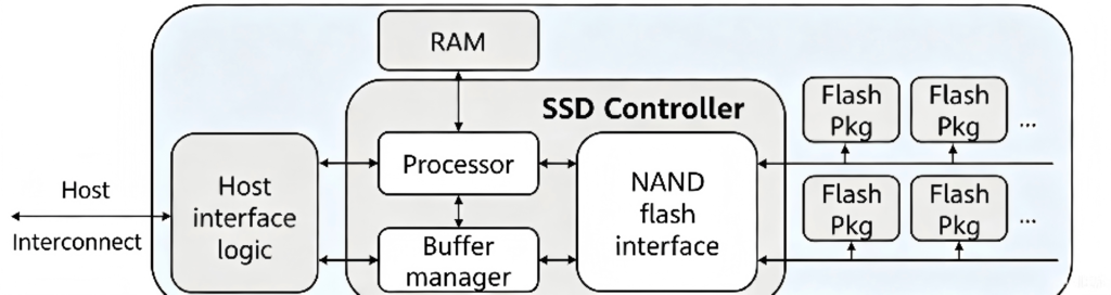
What causes this? Let’s look at the hardware composition of an SSD.
NVMe SSD Storage Speed Limitation for High-Speed RF Data
In reality, all these drives use NAND flash as the actual storage units.
The number of bits stored per NAND flash cell has been increasing over technology generations. SLC stores one bit per cell, MLC two bits, TLC three bits, QLC four bits.
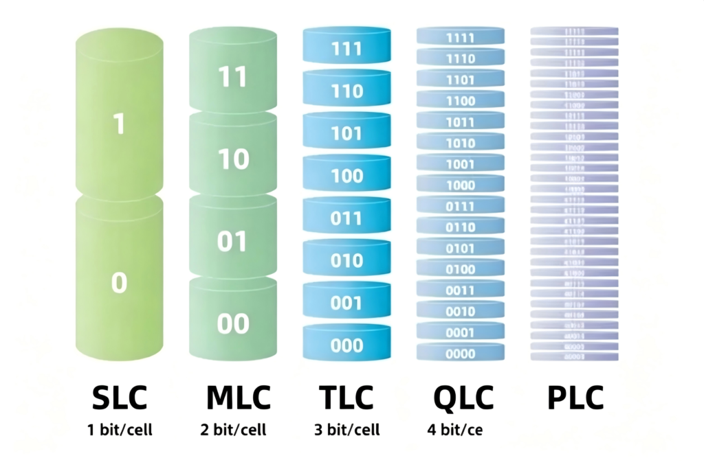
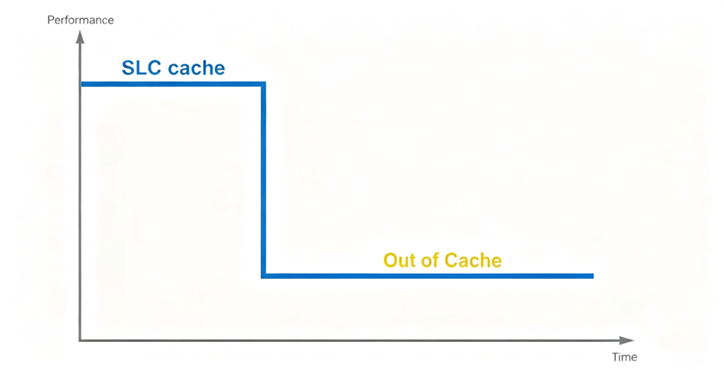
As the number of bits per cell increases, the drive’s capacity naturally grows rapidly, but the write speed decreases. To cope, manufacturers make TLC or QLC drives emulate SLC operation – that is, the cell can actually store 3‑4 bits, but in the emulation state it stores only one bit. In this mode, the write speed is very high – that’s the in‑cache write speed. Once the cache is exhausted, the write mode reverts to true TLC or QLC mode, and the speed drops off a cliff.
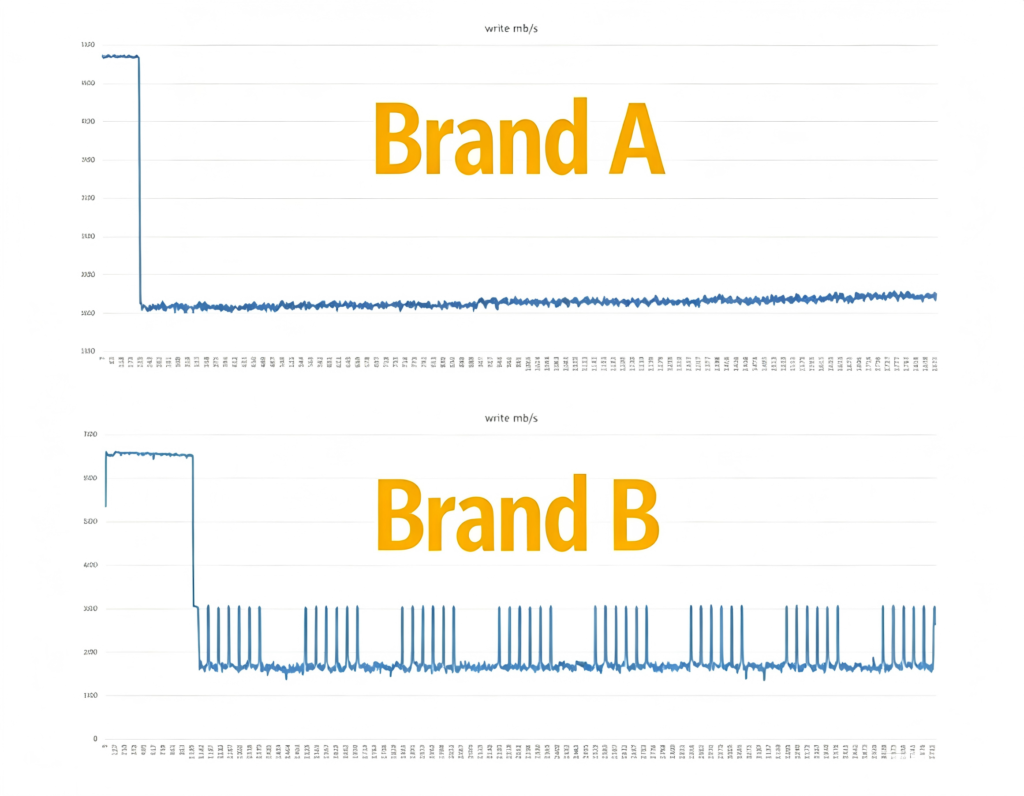
We tested two popular NVMe drives on the market. In both cases, the write speed started very high, but after a few tens of seconds, the out‑of‑cache write speed quickly and sharply declined. To achieve continuous high‑throughput writing of ultra‑wideband signals that fills the entire capacity of the disk array, we must maintain high write speed throughout the whole process. This requires the use of multiple techniques.
High‑performance record‑and‑playback systems typically adopt a modular bus architecture. Whether it’s VPX, PXI, or CPCI, almost all of them use PCI Express (PCIe) as the core data transfer bus. Why PCIe? It has several advantages: very high speed, low latency, and most importantly, a rich commercial ecosystem. For example, the fastest SSDs (NVMe) are all built on PCIe.
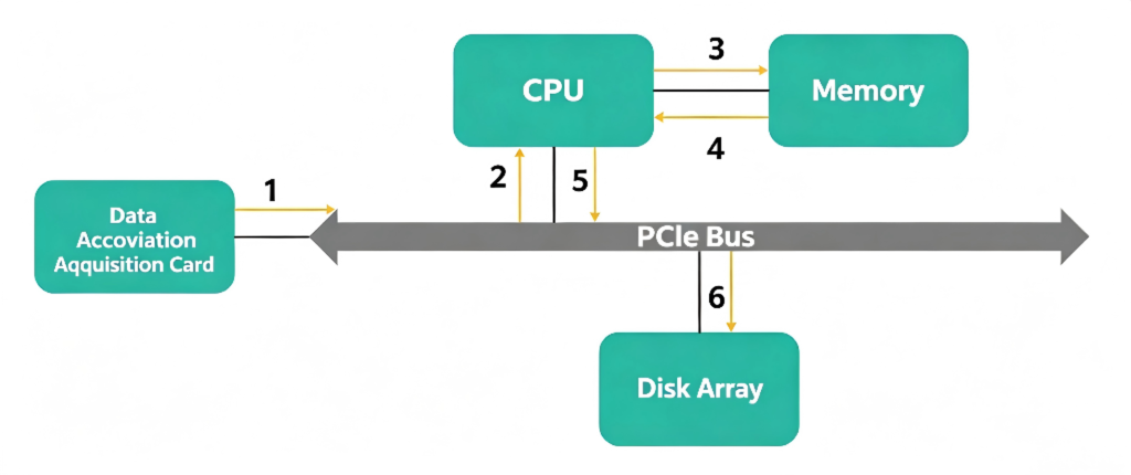
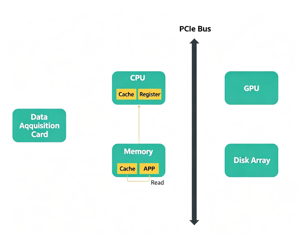
The data acquisition and storage process works like this: after the data acquisition card captures data, it transfers the data over the PCIe bus to the CPU, which then places it into memory. In the application, we need to move the data from kernel‑space memory (used by the driver) to user‑space memory via the CPU – this also goes over the PCIe bus. After processing, we transfer the data over the PCIe bus to the disk for writing. If there is additional signal processing – for instance, using a GPU – there is also a transfer from the CPU to the GPU over the PCIe bus. Thus, the PCIe bus handles most of the data transfers, and each transfer goes through CPU scheduling.
The speed of the PCIe bus is mainly determined by two parameters: the number of PCIe lanes, and the PCIe generation.
Ultra-Wideband RF Record & Playback: PCIe Bus Bottleneck in Multi-channel RF Test System
Currently, PCIe Gen 1 through Gen 5 are available on the market. The number of PCIe lanes is like the number of lanes on a highway – more lanes means faster. The PCIe generation is like the speed limit – a higher generation also gives higher speed.
Where does the bottleneck lie? It mainly occurs at the CPU’s PCIe interface.
Typical consumer CPUs have no more than 16 PCIe lanes.
Even commercial CPUs have only 32‑48 PCIe lanes. In industrial systems, the most common PCIe bus is Gen 3, and the CPU side typically has at most 24 PCIe lanes.
The theoretical speed is only 24 GB per second, and in practice it is difficult to exceed 21 GB per second due to protocol encoding, bus arbitration, and bus multiplexing – all of which affect PCIe efficiency.
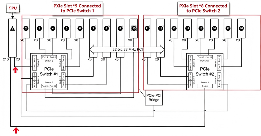
Moreover, high‑speed record‑and‑playback systems usually require multiple slots for AD modules, DA modules, RF front‑end modules, signal processing modules, and disk array modules. Take a PXIe system as an example. The most common slots each use at most a PCIe Gen 3 x8 link, with a theoretical speed of 8 GB per second, but in practice it is hard to exceed 7 GB per second. For a system with more slots – say, an 18‑slot PXIe chassis – there are 17 slots using PCIe Gen 3 x8 links. How are all these slots connected to the CPU? The chassis uses PCIe switch chips to expand the number of PCIe buses. Typically, two PCIe switches are used, each connected to the CPU via upstream links of PCIe Gen 3 x8 and x16, and the downstream side is split into 17 PCIe Gen 3 x8 links. This is like “all roads lead to Rome,” but they all end up squeezed onto two roads – the bus throughput naturally becomes insufficient. For example, suppose in this diagram slot 2 and slot 3 are both AD cards. If both cards send and receive data at full PCIe Gen 3 x8 rates, the upstream link of the PCIe switch is at most PCIe Gen 3 x8, so the data from the two cards will inevitably experience congestion. Therefore, in such large systems, the PCIe bus on the CPU side becomes a major bottleneck for multi‑channel high‑speed record‑and‑playback.
Ultra-Wideband RF Record & Playback: System Memory Bottleneck
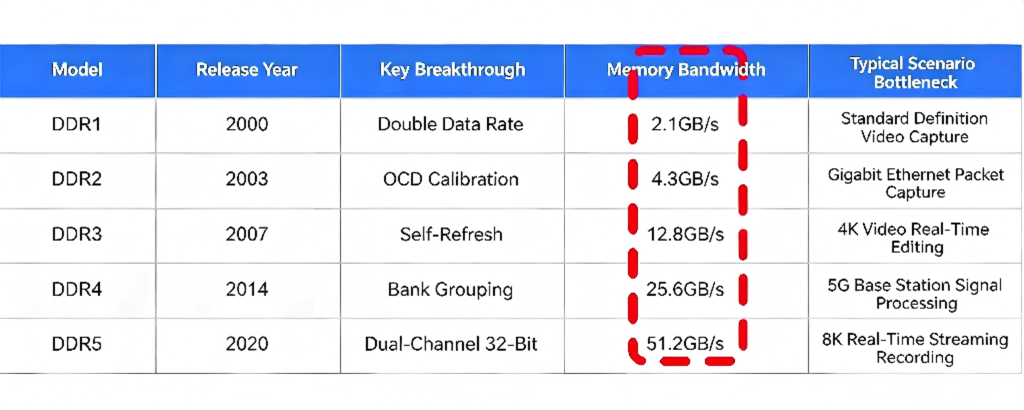
Memory is the fastest storage medium in a computer. Could it also become a system bottleneck? For ultra‑wideband signal record‑and‑playback applications, the answer is yes. Let’s look at the evolution of memory technology. Common memory types on the market range from DDR1 to DDR5, each with different typical bandwidths.
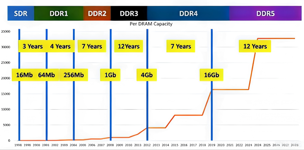
For example, DDR1 memory has an access speed of about 2.1 GB per second; DDR2, about 4.3 GB/s; DDR3, 12.8 GB/s; DDR4, 25.6 GB/s; DDR5, 51.2 GB/s. Dual‑channel or quad‑channel memory can double or quadruple that bandwidth, far exceeding the data rate of ultra‑wideband signal recording. So why does memory become a bottleneck?
We need to look at the entire data flow from acquisition to storage.
Step 1: The acquisition card quantizes the data. We transfer the data from the card into memory via DMA – but this is done by the driver, and the memory used by the driver is typically kernel‑space memory. We then need to process the signal in the application, which involves moving the data from kernel space to application memory space. Each signal processing step generates memory copies.
For example, multiplying or adding signals, or any other operation, requires one memory read and one memory write. If we use a coprocessor such as a GPU or FPGA, we must copy the data from main memory to the GPU’s video memory, then after processing, copy it back from GPU memory to application memory. Finally, after processing, we read the data from application memory and write it to the disk array.
Thus, during this process, the data is read from and written to memory many times. In typical high‑speed record‑and‑playback systems, this reading and writing occurs at least three or four times, sometimes more. At that point, the raw data rate of 8‑10 GB per second multiplies several times, reaching tens of GB per second. Naturally, memory becomes a bottleneck.
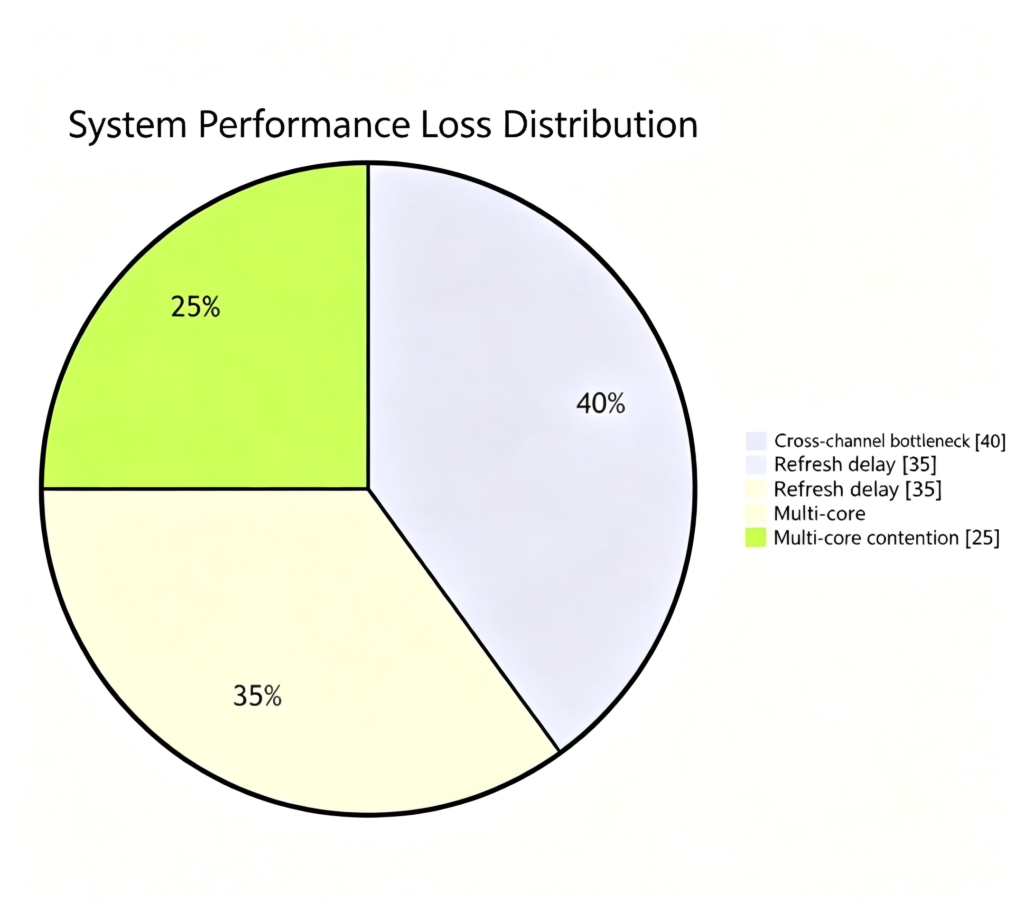
Additionally, memory suffers from refresh latency, CPU multi‑core contention, and cross‑channel bottlenecks – all of which reduce memory efficiency. Therefore, in ultra‑wideband signal record‑and‑playback, memory is also a bottleneck and a challenge.